Explore the latest trends and challenges in PCB manufacturing as of 2021, focusing on key technologies and market demands.
Trends and Technologies in PCB Production
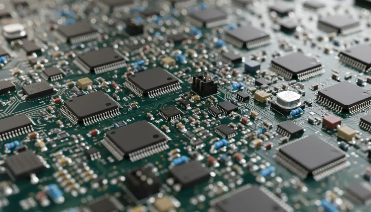
PCB (Printed Circuit Board) technology plays a crucial role across various industries. As of 2021, the PCB manufacturing sector faces a mix of challenges and opportunities. 1. Product Segmentation:- Demand for HDI (High-Density Interconnection) and FPCB (Flexible Printed Circuit Board) has remained lower than anticipated.
- Conversely, there is a robust demand for high-level digital boards and premium packaging substrates.
- There is a growing need for PCBs in smartphones and automotive electronics.
- Strong demand is also present in communication base stations, servers, and computers.
- The value of traditional PCB manufacturing hubs like Japan and South Korea has been declining in recent years.
- However, despite a downturn in mainland China due to COVID-19 in 2020, the region has shown signs of recovery since then.
- PCB technology is evaluated based on criteria such as minimum trace width/spacing, minimum hole/pad diameter, maximum/minimum dielectric thickness, the thickness of copper layers, pad spacing, impedance control, and dimensional tolerances.
How PCB Manufacturing Works
The PCB production process is intricate and comprises several stages:- Design Phase: The design of the PCB determines the functionality of the electronic circuit.
- Material Selection: This involves deciding on the materials used for the PCB, typically fiberglass materials like FR-4.
- Production Phase: The layers of the PCB are assembled, holes are drilled, and copper pathways are created.
- Testing Phase: The functionality of the produced PCBs is tested, and defective ones are removed.
- High productivity and quick production cycles.
- Customization options and adaptability for various applications.
- Advanced technologies allow for thinner circuits and increased component placements.
- High costs and complex manufacturing processes.
- Some manufacturing methods are not environmentally friendly.
- The fast-paced market requires continuous innovation.