Explore PCB packages, their classifications, and how they impact electronic design and functionality.
What Are PCB Packages?
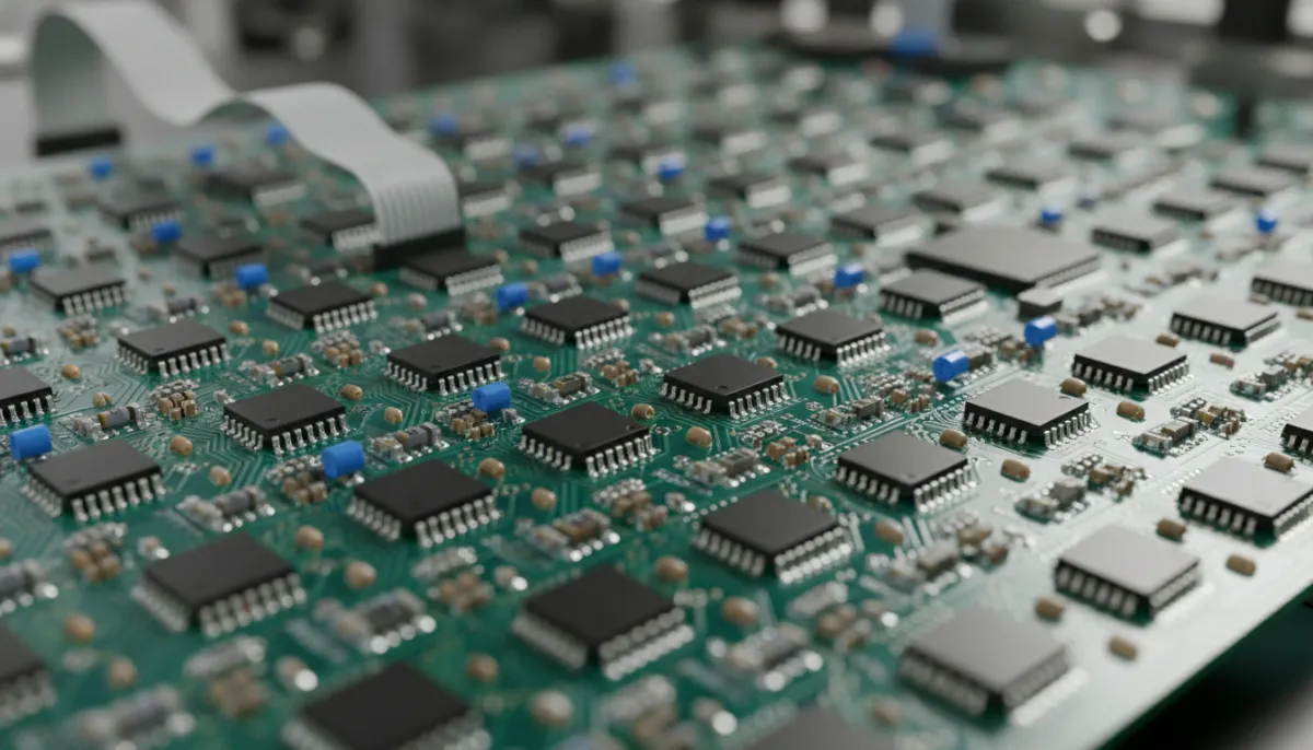
PCB packages serve as the graphical representation of various electronic components, detailing aspects such as size, length, width, level, pad size, and pin dimensions (length, width, and spacing). This definition is designed for use when drawing a PCB diagram.
PCB packages can be categorized based on several criteria, including assembly method, functionality, and device shape.
Classification of PCB Packages
PCB packages can be classified according to their assembly method as follows:
- Mounted Devices: Typically consist of components that are surface-mounted.
- Plug-in Devices: Devices designed to be inserted into the PCB.
- Mixed Devices: These include a combination of both mounted and plug-in components.
- Specialized Devices: Often designed for specific functions or applications and are commonly referred to as through-hole devices.
Based on function and device shape, PCB packages can be divided into the following categories:
- SMD (Surface Mount Devices): Components specifically designed for surface mounting.
- RA (Resistor Arrays): Components that contain multiple resistors.
- MELF: Metal electrode leadless components.
- SOT: Small outline transistors.
These classifications assist PCB designers and engineers in selecting the most appropriate type of components for their projects.
How Do They Work?PCB packages play a pivotal role during the placement of various components onto a PCB. For instance, SMD components are typically placed using automated machines, while plug-in components may be positioned manually or with semi-automatic machines. This process is critical for ensuring accurate component placement and the reliability of connections.
In PCB design, engineers must consider the characteristics of PCB packages when determining the positions, types, and connection points of components. This consideration greatly influences the overall performance and functionality of the circuit board.
Advantages and DisadvantagesAdvantages:
- Efficiency: Modern SMD technology allows for more components to be placed in a smaller area.
- Space Saving: PCB packages save space and facilitate more compact designs.
- Automation: SMD components can be quickly mounted using automated placement machines.
Disadvantages:
- Repair Difficulty: SMD components are generally harder to repair than plug-in components.
- Heat Management: More components in a smaller area can lead to heating issues.
- Special Equipment Requirement: Specialized machines and equipment are necessary for SMD assembly.
- What is a PCB package? PCB packages are graphical representations that convey information about the sizes and positions of electronic components.
- Why are PCB packages important? Correct packages enable proper component placement and enhance the efficiency of the circuit board.
- What is the difference between SMD and plug-in components? SMD components are designed for surface mounting, while plug-in components are intended for insertion into the PCB.
- How should PCB packages be selected? Selection should be based on design requirements, space limitations, and functionality.
PCB packages are essential in modern electronics design and manufacturing, playing a crucial role in optimizing performance and efficiency.